About INFAB Semiconductor
Incubated at CeNSE, Indian Institute of Science (IISc), Bangalore, INFAB Semiconductor Pvt. Ltd. is a pioneering technology company specializing in the design, development, and high-precision manufacturing of advanced MEMS sensors, actuators, and microfluidic chips.
From custom MEMS pressure transducers for aerospace programs to custom glass-bonding mRNA chips for pharmaceutical research, we deliver international-standard deep-tech solutions engineered entirely in India.
Innovation
Proprietary MEMS and microfluidics design IP.
Quality
Strict semiconductor standards & aerospace testing.
Impact
Solving complex fluidic and physical sensing challenges.
Indian Deep-Tech Incubatee at CeNSE IISc
Core Market Domains Serviced
Indigenous Design & IP Portfolio
Institutional & Government Partners
Market Domains & Solutions
We bridge the gap between complex semiconductor physics and functional hardware for mission-critical industries.

Aerospace & Defense
Custom-engineered MEMS products optimized for commercial aircraft, rockets, defense systems, and extreme environment deployments.
- Pressure Switches
- MEMS Pressure Transducers
- Differential Pressure Switches
- Flow Transmitters & Hall Sensors
Semiconductor Fab Services
Foundry process integration and rapid prototyping services utilizing advanced lithography, etching, deposition, and material bonding.
- Custom MEMS Fabrication
- Silicon, Glass, and Polymer Processing
- Special Glass-to-Glass/Si Bonding
- Cleanroom Packaging & Metrology
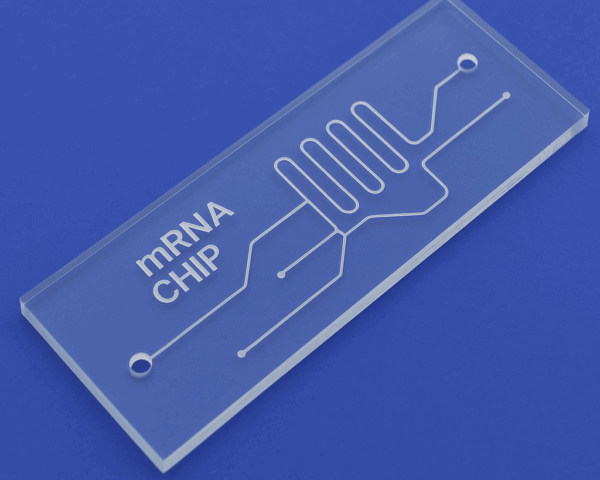
Healthcare & Biotech
Microfluidic chips and fluid control systems designed for organ-on-chip models, droplet generation, cell sorting, and mRNA nanoparticles.
- Microfluidic Chips (Glass, PDMS, PMMA)
- Pressure Controllers
- High-Precision Flow Sensors
- Organ-on-a-chip & Droplet Chips
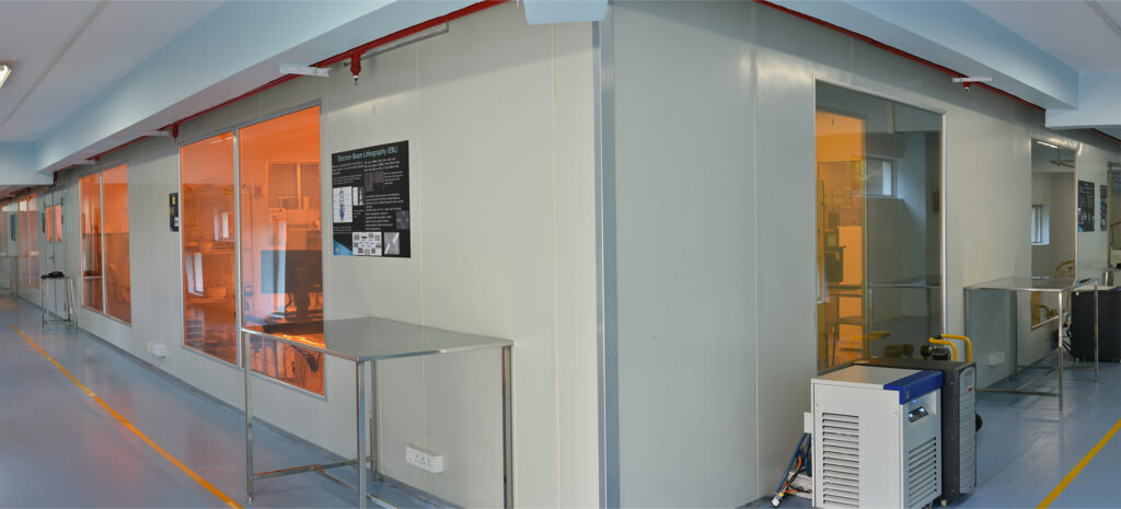
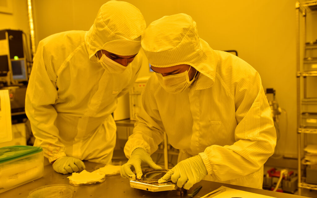
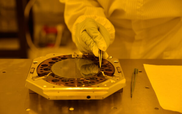
State-of-the-Art MEMS & Microfluidic Fab
Our primary development facilities leverage the world-class cleanrooms at **CeNSE (Centre for Nano Science and Engineering), IISc Bangalore**. This partnership enables us to utilize class 100/1000 cleanroom environments, state-of-the-art electron-beam lithography, photolithography, deep reactive-ion etching (DRIE), thermal oxidation, physical vapor deposition (PVD), and advanced metrology tools.
By combining academic-grade nanofabrication infrastructure with our proprietary commercial packaging, bonding, and quality assurance workflows, INFAB delivers defense-grade micro-sensors and biotech-ready microfluidic products.
Supported By & Incubated At


Trusted By Leading Entities


Let's Discuss Your Project
Whether you need qualified aerospace pressure sensors, a custom-designed organ-on-chip module, or foundry access for MEMS prototyping, our engineering team is here to assist.
Corporate Office & Lab
889/1435, 11th Cross Rd, MCECHS Layout Phase 2, Jakkur, Bengaluru, Karnataka 560064
Incubation Lab
InCeNSE @ CeNSE, Indian Institute of Science (IISc), Bangalore 560012